▲ 213 points
back
113 comments
So many misconceptions here about DRAM. DRAM is miraculously cheap. The process probably costs about $1.50 to $2 per GB, the rest is indeed profit. That nets them maybe $4,000 per wafer - and that includes all the testing, slicing, packaging etc. An average CPU chip in your laptop is about the same size as maybe 3 DRAM chips which cost around $20.
DRAM runs on a separate process which is dominated by the difficulty of building the capacitors. These are roughly the shape of a pencil (long narrow hexagons) where the central structure which holds the capacitor needs to be etched to perfection in a process that can take days. The transistors underneath are, at that scale, about as large as the chad from a paper hole punch. The capacitors are just about as narrow as material science (limit to voltage arcing through the insulation layers) can make them so there is glacially slow progress in shrinking DRAM further. Meanwhile the transistors are at extreme limits of resolution for liquid immersion processing, as also are the lines needed to join the rows and columns. Getting those perfect requires very specialized and competent processing.
They are not easy, second rate circuits. They are a completely separate branch of the silicon world. Unfortunately since they don't scale much any more, current design methods were mature 8 years ago, the only way you get more of them is to build new factories. That means it is a seller's market in a game where building another fab costs $10B and will only succeed if staffed by really expert people. So, it is generally profitable. The 3 vendors cannot easily undercut each other since they all have roughly the same limits, and any attempt to flood the market takes 4 years to build and everyone can see it coming.
So there you are. DRAM is the pivotal technology of the current computer era. Fixing that will most likely require breakthroughs in fundamental memory technology - or a reason for demand to collapse.
>Combined with die stacking, which allows for up to 8 dies to be stacked as a single chip, then a 40 element LRDIMM can reach an effective memory capacity of 2TB. Or for the more humble unbuffered DIMM, this would mean we’ll eventually see DIMM capacities reach 128GB for your typical dual rank configuration.
So on 8 Channel 16 DIMM per socket you could fit a theoretical 32TB of memory. This is insane amount of memory and great for In-Memory Database. ( How is Intel Optane going to compete? )
This makes me wonder, what makes DRAM so expensive? It is still hovering at a median price or around $3/GB compared to NAND which is less than $0.1/GB.
> This makes me wonder, what makes DRAM so expensive?
Greed does. DRAM makers were antitrust busted at least 7 times on my memory in Taiwan, Korea, and USA.
The processes to form NAND and DRAM are completely different. DRAM relies on creating non-leaking capacitors which are highly difficult to manufacture at such a small scale. NAND benefits from innovations in the CPU lithography space since it's essentially all transistor based. Why would you expect them to have the same price, unless you knew nothing about the technology? Also, there are plenty of distinct competitors in the DRAM space. Do you have a source suggesting Micron and Samsung are engaging in price fixing together?
If that's the only reason, then you'd think companies like Apple with dedicated fab timeshare could cut costs by printing their own RAM chips, rather than buying them. And It's not like DRAM contains any complex IP they'd need to license—if you can lay out a CPU, you can lay out RAM.
Add the European Union, Infineon.
[0] https://www.finanznachrichten.de/nachrichten-2010-05/1694023...
This is why even though memory was becoming dirt cheap, prices started to spike in the last few years. There are also less manufactures now as a result of buyouts and mergers.
I'm not an expert, but my understanding of it is that DRAM is mostly just banks of capacitors with some transistors to control when they get recharged or drained. Making capacitors smaller is problematic, because it would decrease the capacitance and require more frequent updates to prevent data loss. So, DRAM doesn't really benefit as much from process shrinks as CPUs do. DRAM does get better and cheaper over time, but the physical constraints on the problem are different.
You would need a new CPU that doesn't yet exist to address 32TB of memory per socket. Existing parts can address 4TB. x86-64 has an ultimate system limit of 256TB, due to its 48-bit virtual address space.
Also worth considering that 32TB of DRAM would draw over 12kW, just sitting there.
> How is Intel Optane going to compete?
You should see how fast Optane will copy a project folder full of node_modules, bin, etc.. Blows the doors off an Evo Plus.
That said, probably not worth the premium for the vast majority of uses.
Is anyone here in the industry? Is there any new tech or process on the horizon that could bring down the price of DRAM?
You can do static RAM this way eg cache but off chip is dynamic ram which is a slightly different process as it uses very small capacitance to store the charge, I also think mixing the two processes on one die is the issue cache is so small relative to dram
you can already have 128gb per DIMM with DDR4. not sure if its up to spec, but it works usually.
128gb dimms are more than double the price of 64gb dimms, so it not always economically viable unless you need max memory density.
> Intel Optane going to compete
Price ;=)
Also Optan drives (over PCI) are probably still interesting for some applications due to low latencies as far as I remember.
Part of it is that the demand isn’t there for extreme densities. Producers are focussing on speed.
Look at base ram in MacBooks, the growth over time is pretty slow.
To the best of my knowledge: with (non-volatile) NAND; 1ms response times vs (volatile) DRAM; 1ns response times... For context; there's 1 million ns in 1 ms. They're in completely different leagues in terms of speed and they're used for very different applications.
While both benefit greatly from economy of scale; the manufacturing tolerances, equipment, etc etc used influences pricing; but I'm not an engineer... so maybe someone here can chime in on that :)
>All the while, there are several smaller changes [...], such as [...] on-die ECC
This means we don't have to worry about ECC support by CPU/motherboard anymore, right?
The author clarifies on-die ECC in the comment section:
> So on-die ECC is a bit of a mixed-blessing. To answer the big question in the gallery, on-die ECC is not a replacement for DIMM-wide ECC.
> On-die ECC is to improve the reliability of individual chips. Between the number of bits per chip getting quite high, and newer nodes getting successively harder to develop, the odds of a single-bit error is getting uncomfortably high. So on-die ECC is meant to counter that, by transparently dealing with single-bit errors.
> It's similar in concept to error correction on SSDs (NAND): the error rate is high enough that a modern TLC SSD without error correction would be unusable without it. Otherwise if your chips had to be perfect, these ultra-fine processes would never yield well enough to be usable.
> Consequently, DIMM-wide ECC will still be a thing. Which is why in the JEDEC diagram it shows an LRDIMM with 20 memory packages. That's 10 chips (2 ranks) per channel, with 5 chips per rank. The 5th chip is to provide ECC. Since the channel is narrower, you now need an extra memory chip for every 4 chips rather than every 8 like DDR4.
I don't assume anything. Intel may find a way to deliberately cripple ECC in the memory controller.
I wonder if this spec increases or decrease memory access latency. The article doesn’t say, which makes me suspicious.
After all, DDR4 has higher latency than DDR3 running at the same clock speed.
That is generally the trade off made to get better clock speeds. And the absolute latency is better with once the speed gets sufficiently fast.
« The big change here is that the command and address bus is being shrunk and partitioned, with the pins being reallocated to the data bus for the second memory channel. Instead of a single 24-bit CA bus, DDR5 will have two 7-bit CA busses, one for each channel »
If there are two 32-bit data busses rather than one 64-bit bus, arithmetic suggests they shouldn't need to find extra pins from somewhere.
So maybe the rationale for shrinking the CA busses (to 7 rather than 12) is something different?
https://images.anandtech.com/doci/15912/DDR5_12.png
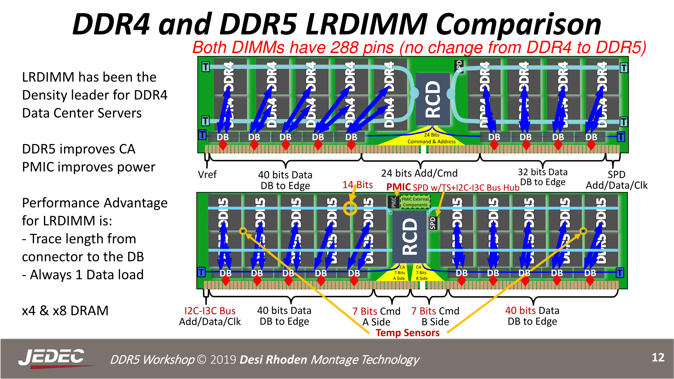
DDR4 appears to have had 40 and 32 bit data buses, while this one has 40/40.
Does this finally address Rowhammer? Ctrl-F on the article yields nothing...
That's more of a die-level issue rather than a module-level issue, isn't it?
Possibly with on-die ECC.
Rowhammer can be eliminated through RAM encryption, e.g. (Transparent) Secure Memory Encryption in Ryzen processors.
How is just splitting the memory in two separate channels going to make anything faster?
How will this affect driver complexity and cache-misses?
This is sort of explained in the article. I think they had to use burst length 16 [1] to scale to 6400 MHz, but 16 * 64 bits would be 128 bytes or two cache lines. The whole memory system works in cache lines, so it wouldn't be good if the processor requested one cache line and got two. So they use BL16 with a narrower 32-bit channel to fetch one 64-byte cache line.
As long as multiple cores are accessing memory or prefetching is on (it's almost always on), both channels will be utilized so software won't notice.
[1] When you do a read operation on DRAM you get a multi-cycle burst of data, not just one word. This amortizes command/address overhead and presumably matches the slow-but-wide internal DRAM array with the fast-but-narrow channel. See https://people.freebsd.org/~lstewart/articles/cpumemory.pdf sec. 2.2.
> How is just splitting the memory in two separate channels going to make anything faster?
I am not a HW engineer, but:
With DDR, the difference of all traces in the same channel (data & clock) has very tight tolerances (on the order of 1/8 or 1/16 of a clock). Having fewer traces per channel may make it easier to route for higher clock speeds.
> How will this affect driver complexity and cache-misses?
I'm not sure what you mean? The memory controller should abstract almost all of the differences away. There are per-channel configuration settings that are usually configured by the SPD rom, so there will be twice as many to set, but multichannel memory controllers are already a thing, and going from N to 2N of something doesn't really affect software complexity once N is greater than one.
you can issue two commands simultaneously. yes, the data transfer latency takes twice as long in theory, due to the bus size halving, but with increased clock speeds its not really an issue.
Similarly to how dual channel memory is faster than single channel. Now you can do dual channel with a single stick, or maybe even quad channel with 2 sticks. I believe it should be otherwise transparent to the rest of the system.
Are there any changes in there for bulk memory operations such as copying or zeroing?
Wonder if this spec will make it easy for embedded systems to catch up. It always seems like they lag behind what's cutting edge. Maybe that's a cost/benefit analysis.
I have a brand new design with DDR2. I can power memory from existing 1.8V rail, no need for more voltage regulators. And 400 MHz is totally ok for me since I can have whole memory bandwidth for myself, no operating system, etc. And my application is very cutting edge for sure in its domain.
Both DDR4 and DDR5 have the same 288 pinout. Hopefully nothing bad happens if a stick is plugged into the wrong socket.
Same pin count, but different keying provides a mechanical barrier against inserting the wrong kind of module.
> Both DDR4 and DDR5 have the same 288 pinout.
The article is actually explicit of this not being the case:
DDR5 DIMMs: Still 288 Pins, But Changed PinoutsThere's a notch in the slot that can be changed.
They'll change the keying so that that can't happen. Same as with DDR2 and DDR3
Why not QDR2?
Despite sounding related, QDR and DDR are mostly unrelated technologies. They are also both poorly named.
The real purpose of DDR is not actually to double the data rate, but to halve your clock speed and allow you to use the same frequency for your clock as your data. This mostly benefits signal integrity.
QDR is better understood as memory with two ports, one for reading and one for writing, which can be used at the same time. This is a lot more expensive and really doesn't have huge benefits for PCs compared to just adding more channels (as DDR5 does).
so, will we see mini-ITX mobos that support 128Gb RAM?
Yes, although maybe not soon.
This may be a stupid point, but, for personal use of computers in their current form, how much memory do you really need? I’m still a little baffled why chrome requires GBs of memory...? Can we have lean software please?
In a word: No.
CPUs have become so fast that relative to their "internal" speeds, RAM is the new hard disk. Databases are becoming in-memory, and going out to fixed storage, even SSD, is an anathema.
New applications are not designed to work on data sets bigger than physical memory. Disk-to-disk streaming algorithms are practically unheard of outside of a few niche scenarios. Like I said, even database vendors are moving to in-memory!
I love machines with huge amounts of memory. My laptop has 64 GB, and it's great! I can run entire fleets of servers in a local hypervisor. I can load huge blobs of CSV or JSON data into the shell and not have to worry about the 2-5x overhead of the in-memory representation. It'll fit just fine. I can run every "bloated" app at once and still have 50 GB free for "whatever". I've reindexed a database on my laptop in minutes that would have taken days(!) on a production server because it didn't have enough RAM and was thrashing the storage like crazy.
Another way to look at it is the "GB per CPU core". With existing AMD EPYC 2 CPUs having 64 cores and 128 threads, the typical 512 GB memory configuration is "only" 8 GB per core, or 4 GB per thread! With a dual-socket server, halve those numbers again. Similarly, mainstream desktop Ryzen CPUs have up to 16 cores, and that's not even talking about the not-so-mainstream Threadripper line. For 4GB per core, you'd need 64 GB.
It's likely that AMD will release 24 or 32 core mainstream CPUs in the near future, maybe as soon as 2 years from now when their 5nm products start shipping. I fully expect server CPUs to hit 96-128 cores per socket around the same time frame, or up to 512 hardware threads in a standard two-socket server. Terabytes of memory is going to become "standard" very soon now.
People always mention more memory usage as a bad thing, but with Moore's Law slowing down, we are being forced to find other ways to speed up computation. One of those ways is trading memory usage for performance via look up tables, caching, duplication, less compact data storage, etc. I would expect memory usage to rise significantly as long as memory technology advances quickly while clockspeeds remain flat.
Based on what's on my existing system I think I could benefit from ~1TB of memory. Above that I'd have to probably try. After maybe ~200GB I bet I'd start to see seriously diminishing returns.
My servers could probably benefit from, idk, petabytes? If I could keep the entirety of my server's hard drive in RAM I'd be very happy.