▲ 392 points
back
205 comments
> logic technology can extend for the first time below the 1 nm node, advancing the era of angstrom-level scaling, where dimensions approach the size of individual atoms. While transistor nodes now refer to a generation of manufacturing technology versus an exact physical dimension, IBM’s 0.7 nm technology—also referred to as 7 angstroms—demonstrates how continued scaling remains possible.
Continuing the well established trend of making bold claims about physical dimensions that have nothing to do with any of the structures in the chip, and the name scales better than the tech.
What they actually deliver is a "nanostack architecture" built with ~5nm features that according to them is comparable to a hypothetical real sub-1nm chip.
It's an impressive achievement nonetheless but it looks like the industry has a few too many marketers.
As it can be seen from the photos, horizontally the features are much bigger than 5 nm.
For silicon, the gate length of a FET has a lower limit somewhere between 10 nm and 15 nm.
The current CMOS manufacturing processes have not reached the limit yet. For making smaller transistors, a transition to other semiconductor materials will be necessary.
The vertical thicknesses of various layers may be of only a few nanometers or even of a fraction of a nanometer, but that does not matter directly for the circuit density.
The supposed node size refers to horizontal dimensions, not to vertical dimensions.
Vertical dimensions of around 1 nanometer or less could be achieved already many decades ago, because they depend on growth speed and on time, not on lithography, like the horizontal dimensions.
The industry should have stopped decades ago to talk about the "size" but they should have characterized a CMOS process by its density, e.g. in logic gates per square mm.
However, an actual concrete number would be disliked by marketing, because they could no longer claim that their "1 nm" process is better than the "2 nm" process of another vendor, if their density is not really better.
Unlike marketing terms, "nm density" is actually useful measure.
It describes density measure where you can compare it to planar transistors from the 28-nanometer (28 nm) node around 2010 to 2011 and before. A "0.7 nm" node has equivalent transistor density as if we could have shrunk standard flat transistor node down to 0.7 nanometers.
It's been decades since published node sizes had any connection to actual feature size. Sadly this is just how it works in the semiconductor industry now.
My read on it was that they are trying to imply a transistor density (in a 2D plane sense) that is comparable to a 1nm process? But they achieve that through stacking (3D, not 2D) since the features aren't actually anywhere near 1nm?
Better metrics are transistors/mm^2, performance/watt, and raw performance, since at this point "nm" is fluff and easily game-able.
Different companies measure it differently too. This was a while ago, but I remember reading that Intel 10nm was more or less close to TSMC 7nm. I'm sure this is still true to varying degrees.
> Continuing the well established trend of making bold claims about physical dimensions that have nothing to do with any of the structures in the chip, and the name scales better than the tech.
We care about PPA (power, performance, area) and not how large or not-large features actually are. Comparing gate lengths between a 1980s planar transistor and a 2010s 3D FinFET or GAA transistor is obviously nonsense, the relatively aligned node names of the industry actually do make sense as a shortcut here.
yeah, where on the pictures is the 0.7nm feature?
The linespacing is around 5nm. Is it the white line which is 0.7nm?
On the otherhand, no investor really cares what it's called, they just need to know it's next gen.
What industry doesn't have a few too many marketers? Take everything with a grain of salt.
only a matter of time before some marketer figures out they can get promoted by branding a generation of chips 0nm
I believe it could be a stepping stone to significantly higher density in the future.
Just to be clear, this doesn't mean that anything on the die actually measures 0.7nm — it means that it's roughly double the density as the previous node generation. At some point the industry decided to keep talking about "nanometers" even though the actual transistor sizes have been decoupled from the node name for years.
Generations.
Gen Alpha were born since the naming became detached from actual physical size. And parts of Gen Z (before) and Gen Beta (after).
For what it's worth, here's my 7000+ word deep dive into the technology.
https://morethanmoore.substack.com/p/ibms-announces-07nm-pro...
Hi Dr. Cutress! I loved reading your deep dives on Anand, they're what got me interested in semiconductors. Hope you're well <3
weird q: the photo shows a wafer with partial chips rendered on the edges?
Two big problems 1) NOBODY knows what IBM's definition of "sub 1nm" means 2) IBM bullshits so much more than anyone including Intel (remember the "teleportation" ads years ago) that nobody is going to waste time researching what they mean in reality
> remember the "teleportation" ads years ago
Never heard of this, care to elaborate?
Maybe it is done to pump their stock with low effort? It seems that way for many companies.
The most surprising part for me is that IBM still somehow owns silicon labs, I was sure it's effectively a consulting company by now
Remember that IBM paid Global Foundries $1.5 billion to take their fabs and design services group.
GF did not pay IBM. IBM paid GF to take the fabs away.
https://www.reuters.com/article/technology/ibm-to-pay-global...
One of the images has "15 rows of Si atoms".
Is there a limit to how small things can go? A single atom?
Is there a physical/molecular limit to Moore's Law?
Looking at this picture: https://filecache.mediaroom.com/mr5mr_ibmnewsroom/201436/IBM...
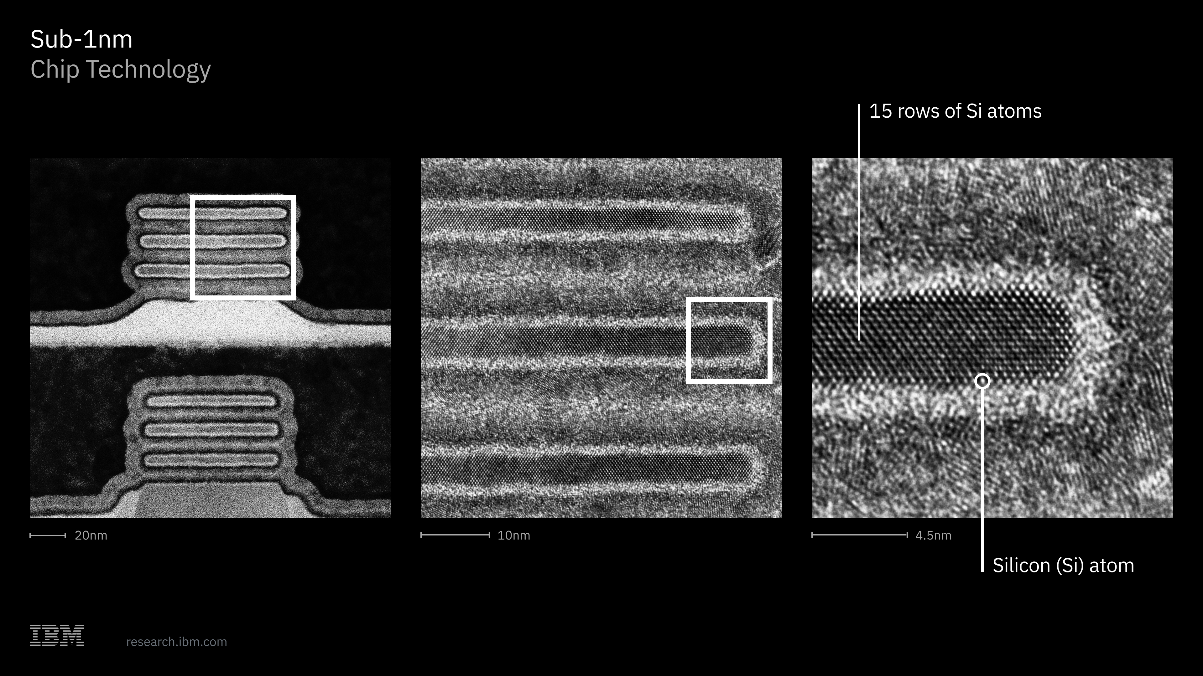
I am just astonished at the quality of the structure. Not only that, but the quality of the "cut" to then be able to take this picture. I was closely involved in EM imaging more than 30 years ago, this is just wonderful to see such pictures now.
Why doesn't the industry use something like transistor density per cubic cm? This would extend to 3d cases and impossible to fake
How does IBM commercialize this? Do they license this out to fabs?
Keep hearing that IBM makes these incredible chips but don’t see anyone using IBM chips. What do they do with them?
For anyone who needs it, a friendly reminder that CPU nm marketing is a complete fabrication and the physical size of transistors has zero relation to the marketing claims. These are not, in fact, physically sub 1 nm, despite the bombastic claims.
> IBM and its partners conduct this work at a leading semiconductor research facility in Albany, New York, which will soon be home to a High Numerical Aperture Extreme Ultraviolet (High NA EUV) lithography tool, essential for the future of logic scaling. Developed by ASML, this technology enables ultra‑precise circuit printing, supporting the creation of smaller, more powerful chips.
I'm guessing that this is the technology that is developed by Cymer (ASML subsidiary) in California, correct? Is there competing technology? I know xLight is trying to make some inroads on their own version of this EUV tech. I have not heard about any progress though.
Relevant quote:
> IBM sees a path to production in as early as the next 5 years.
5 years is a long time for a product roadmap, so there are probably some significant unsolved problems remaining, and the timeline depends on whether IBM can solve these problems.
Physically impossible. I thought process-node marketing terms had already gradually started to drop "nm", like "Intel 7" and so on, which was the old "10nm".
But seeing progress in semiconductor nodes is always a good thing. It has felt quite stagnant these past few years.
What surprised me is that it came from IBM.
How do these 3D architectures scale regarding yield? (The naïve expectation would be that adding vertical layers should have exponential impact on yield.) Is this commercially viable, near term?
I wonder at what point does it become deceptive in the legally biting way to market process nodes like this. One can wax and wane a bunch about industry terminology status quo, but this is mental.
I'm sure this is a wonderful breaktheough but I'd rather have the current, or a recent, generation of semiconductor technology available at a reasonable price.
More marketing lies from IBM.
Sad to see the decline and corruption of a once OK company.
Selling a 5 nm vertically stacked chip as equivalent to 0.7 nm
Shades of Watson and other IBM lies.
Since a transistor can't be smaller than a single atom, maybe it's time to start optimizing our software again.
Is the 3D transistor proposed by IBM on the same track as Tao's Law proposed by Huawei?
IBM regularly announces silicon breakthroughs like this but I'm not aware of those ever becoming products. Is IBM mainly in the business of licensing their technology to big silicon manufacturers with stuff like this? Is it just marketing for their consulting business?
has anyone found a paper with details?
also, I was expecting to see cfets mentioned.
They dont give the exact size hmm
Sub-Atomic level chips soon, then?
IBM debuts a PDK and some test structures, as they have no production fabs
How come we don't hear anything about Watson?
Not bad, now you just have to fold it 86 times to reach one Planck length. The only issue you'd run into is it would have to be 77 quadrillion kilometers thick
A little bit of a nitpick, but wouldn't that be a picometer instead of angstrom node? Like, isn't a "pico-" the next magnitude smaller than "nano-", or am i wrong?
Otherwise, that chip tech sounds really awesome - at least for the future!